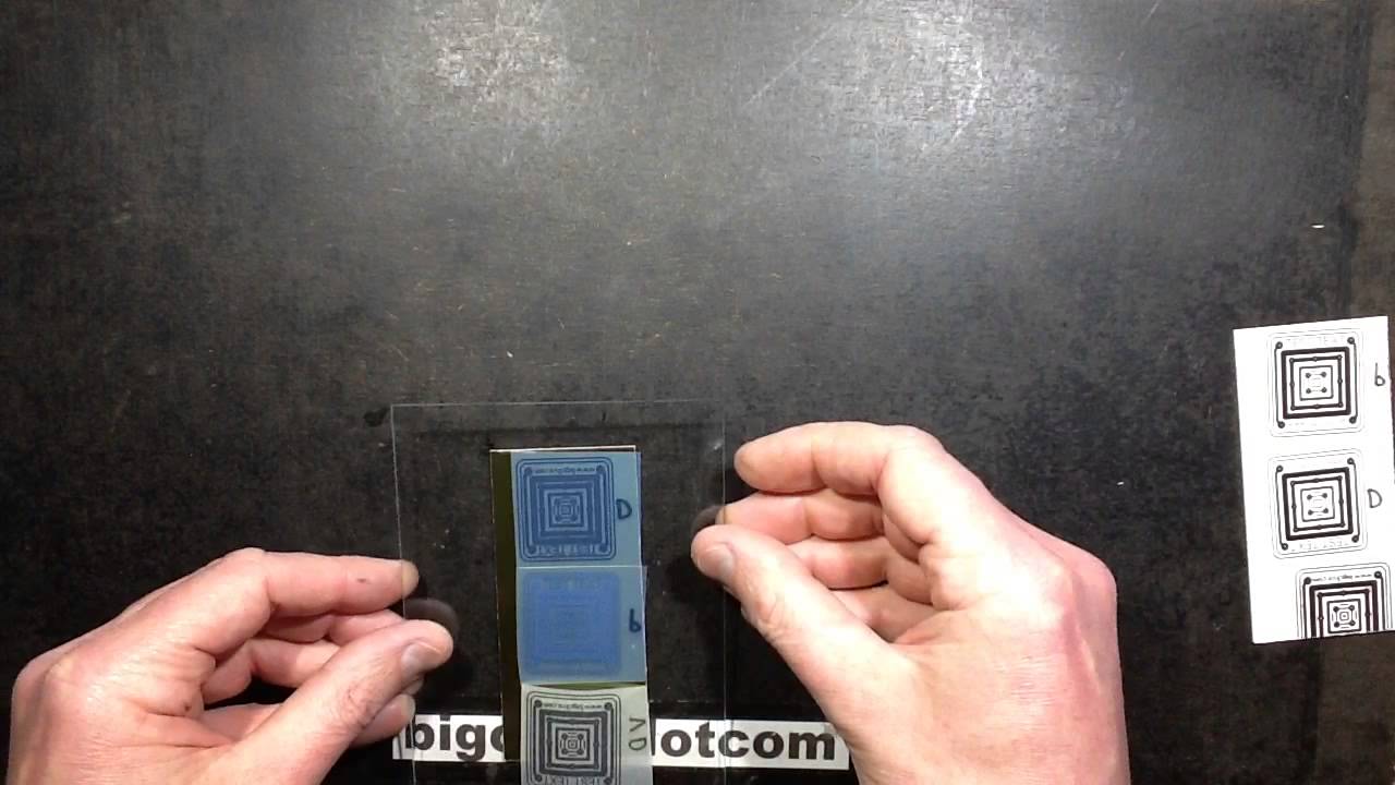
I didn’t realise this material existed up until now. The silkscreen industry uses the same photo transfer techniques as the PCB prototyping industry, but since it’s a much bigger market they have specific transparency materials designed to absorb a LOT of ink deeply from inkjet printers, but still pass UV light for exposing the image.
The material is available on ebay if you search for the keywords:-
inkjet screen printing film
Unlike the traditional overhead projector transparencies that are very clear, the screen printing film is very translucent with a milky opal sheen. This is due to the thicker layer of the coating that absorbs the ink. It absorbs it so well that it comes out the printer virtually touch dry and ready to use. The definition is also super detailed with no bleeding or smudging.
It also seems very resilient to being placed printed side down on the laminate. I had an issue with one of the overhead projector films losing ink and coating onto the PCBs photosensitive layer.
At the same time I also tested a material called inkjet vellum, which is basically a thick tracing paper. It came from an ebay craft seller (search for inkjet vellum) and to my surprise it took the dye based ink very well. It didn’t fare so well with the pigment ink though. I think this is down to the larger particle size of the pigment blocking the papers pores.
Also note that the dye ink has visibly penetrated deeper into the screen printing film than the pigment ink, probably due to the particle size again.
This is all good news. It means that the common dye based ink is actually better suited to making the transparencies with these materials.
Neither of the materials I tested was detectable by the EPSON optical paper detector. I had to feed the sheets through in a carrier sheet with about half an inch (12.5mm) folded at the bottom to grip the film and make it visible to the printer. If you do this, make sure you print well beyond the folded lip to avoid jamming the print-head against the folded area.
In the video I reference the lifespan of the developer solution. I recommend using sodium metasilicate as a developer. You can use common caustic soda (sodium hydroxide) but the latter is more volatile (and destructive) and also has a very short usage life. The sodium metasilicate (water glass) has a very long working life and can be used repeatedly until it slows to the point you want to make new stuff up. The mixing ratio is 12.5g in 250ml of warm water.
As before I used the printers in a forced mode to produce a heavy black image. It was done with the matte photo paper setting and the colours adjusted to cause a high contrast image. Modern printers may have more paper settings that let you specify how much ink is laid down.
Another interesting find during the making of this video is that the cheap ebay ultraviolet nail varnish curers that use a cluster of four fluorescent lamps do a good job of exposing the film, but the built in two minute timer is maybe a bit too long. (It’s hard coded in software.) I’d recommend experimenting in the 1 to 1.5 minute region, although that will depend on the quality of your transparency and the sensitivity of the laminates coating. The cheap ebay unit actually exposes the PCB material faster than my big industrial tubes-in-lid unit.

